Asahi Kasei, a diversified global company, has announced the establishment of a Smart Laboratory, an R&D platform that autonomously performs a series of materials development processes using AI and automation technologies. The new Smart Laboratory is located at the company’s research and manufacturing complex in Fuji City, Shizuoka Prefecture, Japan.
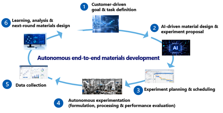
Scheduled to begin operation in January 2027, the Smart Laboratory will be used to develop Pimel™ photosensitive dielectric material for semiconductor applications. At the Smart Laboratory, the entire development cycle will be autonomously repeated within a single integrated experimental system. This spans from material design and experimentation to processing and performance evaluation that simulates customers’ semiconductor packaging processes, as well as incorporation of the results into subsequent material design. By automating the formulation of a wide variety of raw materials for Pimel™ as well as processing and performance evaluation, the Smart Laboratory will be able to increase the number of development experiments to approximately four times the conventional level, as measured by the number of material formulations that can be evaluated within a given period.
In its medium-term management plan “Trailblaze Together,” Asahi Kasei positions Electronics, including Pimel™ and other electronic materials, as a “First Priority” business to drive earnings growth.
Asahi Kasei has leveraged its extensive R&D expertise and robust quality assurance capabilities to rapidly develop Pimel™ material solutions that accurately address customer needs. With the interlayer dielectric materials market expected to maintain a CAGR of approximately 8% through around 2030, Asahi Kasei is further increasing its production capacity to meet rising demand.
As generative AI drives innovation in leading-edge semiconductors, customer expectations continue to rise, posing challenges in terms of achieving multiple performance requirements simultaneously. This makes the product development process more complex with a significant increase in the number of material combinations, experimental conditions, and evaluation parameters to be considered. To anticipate next-generation customer needs and create innovative materials beyond conventional approaches, Asahi Kasei is adopting a new R&D model that enables broader and more efficient exploration of vast development possibilities.
Key features of Asahi Kasei’s Smart Laboratory
1. End-to-end autonomous development
While autonomous experimentation is gaining momentum worldwide, most applications remain limited to specific materials, individual process steps, or academic research. Asahi Kasei’s Smart Laboratory autonomously integrates the entire development cycle within a single experimental platform—from material design and experimentation to evaluation and learning. The system automatically plans and executes experiments, including material formulation, sample preparation, and processing and evaluation that simulate customers’ semiconductor packaging processes. Experimental and evaluation data are continuously fed back into the AI model for learning and analysis, enabling the proposal of subsequent formulations and experimental conditions. By autonomously repeating this cycle of experimentation and learning, the Smart Laboratory significantly expands the number of development experiments, measured by the number of formulations evaluated within a given period.
2. Highly accurate predictions based on extensive proprietary data
The effectiveness of materials informatics (MI) depends heavily on the quality and scale of experimental data. Leveraging a data infrastructure that enables extensive experimental data accumulated through Pimel™ development to be utilized for MI, the system combines newly generated data, public datasets, researchers’ expertise, simulations, and theoretical chemistry. This allows the exploration of new formulations that were previously overlooked by conventional wisdom, with intensive validation of surrounding formulations and conditions while using iterative learning to further enhance predictive accuracy.
The Smart Laboratory will significantly accelerate Pimel™ development by enabling broader exploration of material candidates. This will facilitate new breakthroughs including the discovery of promising new materials capable of achieving demanding and often competing performance requirements, such as fine patterning, dimensional stability, high reliability, and high resolution. By accelerating product development that anticipates the needs of leading-edge semiconductor manufacturers, Asahi Kasei will continue contributing to the advancement of the semiconductor industry.
Moving forward, the R&D capabilities accumulated through the Smart Laboratory for Pimel™ will be applied to other electronic materials and additionally to other businesses in the Material sector. Furthermore, Asahi Kasei will refine the process to achieve development goals through dialogue between researchers and AI, pursuing new possibilities in technology development. By combining researchers’ expertise with AI while leveraging technologies, data, and knowledge group-wide, Asahi Kasei aims to accelerate innovation and create new value in its Healthcare, Homes, and Material sectors.